| CPC G11C 29/026 (2013.01) [G11C 7/065 (2013.01)] | 16 Claims |
|
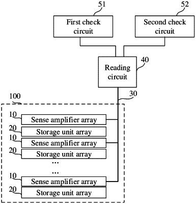
1. A storage device, comprising:
a storage circuit, comprising a plurality of sense amplifier arrays and a plurality of storage unit arrays, the sense amplifier arrays and the storage unit arrays being arranged alternately, and the sense amplifier arrays being configured to read and write data to the storage unit arrays;
a first data wire, electrically connected to each of the sense amplifier arrays;
a reading circuit, electrically connected to the first data wire and configured to read data on the first data wire;
a first check circuit, electrically connected to the reading circuit; and
a second check circuit, electrically connected to the reading circuit; the reading circuit being configured to transmit a part of read data to the first check circuit for error checking and/or correcting, and transmit another part of read data to the second check circuit for error checking and/or correcting,
wherein the data transmitted to the first check circuit and the data transmitted to the second check circuit are respectively from adjacent sense amplifier arrays.
|