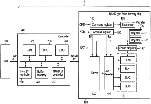
| CPC G11C 16/10 (2013.01) [G06F 3/0604 (2013.01); G06F 3/0659 (2013.01); G06F 3/0679 (2013.01); G11C 11/5628 (2013.01); G11C 11/5635 (2013.01); G11C 16/0483 (2013.01); G11C 16/08 (2013.01); G11C 16/14 (2013.01); G11C 16/32 (2013.01); G11C 16/349 (2013.01); G11C 16/3459 (2013.01); G11C 16/3495 (2013.01); G11C 29/021 (2013.01); G11C 29/028 (2013.01); G11C 29/42 (2013.01); G11C 11/5671 (2013.01); H10B 43/27 (2023.02); H10B 43/35 (2023.02)] | 20 Claims |
|
1. A memory device connectable to a controller, the memory device comprising:
at least a first memory cell configured to be programmed to store data corresponding to a threshold voltage of the first memory cell, the first memory cell being configured to store first data in a case where the threshold voltage of the first memory cell is higher than a first reference voltage; and
a peripheral circuit configured to:
write the first data to the first memory cell in a first programming operation by:
applying a first program voltage to the first memory cell in a plurality of first loops;
obtaining a value of a first write parameter by comparing the threshold voltage of the first memory cell with a second reference voltage, the second reference voltage being lower than the first reference voltage; and
verifying that the first data is stored in the first memory cell by comparing the threshold voltage of the first memory cell with the first reference voltage; and
output the value of the first write parameter to the controller.
|