| CPC G11C 16/0483 (2013.01) [G11C 11/4087 (2013.01); G11C 16/08 (2013.01); H10B 12/30 (2023.02); H10B 41/10 (2023.02); H10B 41/27 (2023.02); H10B 41/35 (2023.02); H10B 43/10 (2023.02); H10B 43/27 (2023.02); H10B 43/35 (2023.02); H10B 80/00 (2023.02)] | 20 Claims |
|
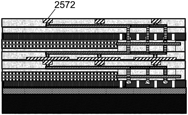
1. A semiconductor device, the device comprising:
a first level comprising a plurality of first memory arrays,
wherein said first level comprises a plurality of first transistors and a plurality of first metal layers;
a second level disposed on top of said first level,
wherein said second level comprises a plurality of second memory arrays;
a third level disposed on top of said second level,
wherein said third level comprises a plurality of third transistors and a plurality of third metal layers,
wherein said third level is bonded to said second level,
wherein said bonded comprises oxide to oxide bonding regions and a plurality of metal to metal bonding regions,
wherein said first level comprises first filled holes,
wherein said second level comprises second filled holes, and
wherein said third level comprises a plurality of decoder circuits.
|