| CPC G11C 11/4093 (2013.01) [G11C 7/1039 (2013.01); G11C 11/4074 (2013.01); G11C 11/4094 (2013.01); G11C 11/4096 (2013.01); G11C 11/40615 (2013.01)] | 20 Claims |
|
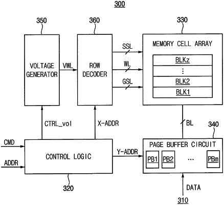
1. A page buffer circuit comprising:
a plurality of page buffers connected to a plurality of bitlines,
wherein each of the plurality of page buffers comprises a bitline selection transistor configured to connect a corresponding bitline of the plurality of bitlines to a sensing node, a precharge circuit configured to precharge the sensing node, and a dynamic latch circuit configured to store data in a storage node,
wherein each of the plurality of page buffers is configured to refresh the data stored in the storage node through charge sharing between the storage node and the sensing node, and
wherein each of the plurality of page buffers is configured to perform a first refresh operation and a second refresh operation to refresh the data stored in the storage node,
the first refresh operation stores inverted data that are inverted from the data in the storage node, and
the second refresh operation stores the data that are inverted from the inverted data in the storage node by using the charge sharing between the storage node and the sensing node.
|