| CPC G11C 11/4087 (2013.01) [G11C 5/10 (2013.01); G11C 11/4023 (2013.01); G11C 11/4097 (2013.01)] | 20 Claims |
|
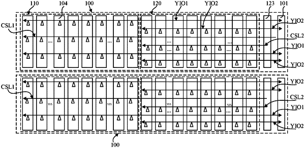
1. A bank, comprising at least one storage module, each of the at least one storage module comprising:
a read-write control circuit, a column decoding circuit, and a plurality of storage arrays arranged along a first direction, the plurality of storage arrays being divided into at least one first unit and at least one second unit, wherein each of the plurality of storage arrays comprises a memory array and a sense amplifier (SA) array, and each SA array is spaced from each memory array in the first direction;
a first decoding selective signal line, the first decoding selective signal line being electrically connected to the column decoding circuit and storage arrays in the first unit;
a second decoding selective signal line, the second decoding selective signal line being electrically connected to the column decoding circuit and storage arrays in the second unit;
a first data signal line, wherein the first data signal line is electrically connected to the read-write control circuit and the storage arrays in the first unit, and the first data signal line spans the storage arrays in the first unit and the storage arrays in the second unit; and
a second data signal line, wherein the second data signal line is electrically connected to the read-write control circuit and the storage arrays in the second unit, and the second data signal line spans the storage arrays in the second unit.
|