| CPC G11C 11/4076 (2013.01) [G11C 11/4093 (2013.01); H03K 3/017 (2013.01); H01L 25/0657 (2013.01); H01L 25/18 (2013.01)] | 20 Claims |
|
1. A semiconductor memory device comprising:
a mode register set configured to store a first control code set received from a memory controller and configured to set an operation mode of the semiconductor memory device; and
a clock correction circuit configured to:
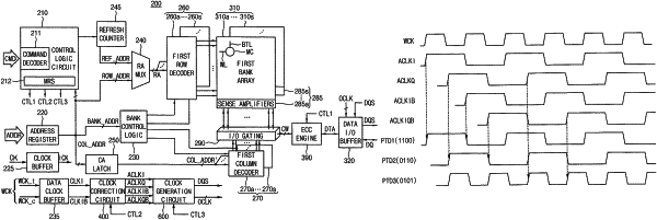
generate first, second, third, and fourth divided clock signals, which have a phase difference of 90 degrees with respect to each other, based on a data clock signal received from the memory controller;
generate first second, third, and fourth adjusted clock signals by adjusting skew of each of the first, second, third, and fourth divided clock signals; and
sequentially perform a first duty cycle training to search a second control code set, a second duty cycle training to search a third control code set, and a third duty cycle training to search the first control code set, during a duty training interval based on a duty training command received from the memory controller,
wherein the second control code set is associated with the first divided clock signal and the third divided clock signal,
wherein the third control code set is associated with the second divided clock signal and the fourth divided clock signal, and
wherein the first control code set is associated with the first divided clock signal and the second divided clock signal.
|