| CPC G11C 11/4074 (2013.01) [G11C 11/4085 (2013.01); H01L 24/08 (2013.01); H01L 25/0652 (2013.01); H01L 25/0657 (2013.01); H01L 25/18 (2013.01); H01L 2224/08146 (2013.01); H01L 2225/0651 (2013.01); H01L 2225/06541 (2013.01); H01L 2924/1427 (2013.01); H01L 2924/1436 (2013.01)] | 19 Claims |
|
1. A semiconductor memory comprising:
a memory chip comprising at least a storage array; and
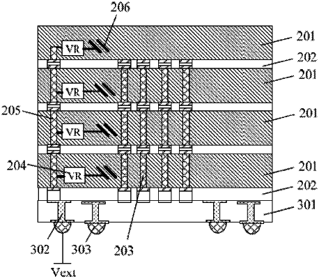
a voltage regulation unit comprising at least an operational amplifier, wherein the voltage regulation unit is configured to convert an external input first voltage into a second voltage to be provided to a word line driver circuit associated with the memory chip, wherein the external input first voltage is greater than the second voltage, wherein the voltage regulation unit is an independent voltage regulation chip, and wherein the semiconductor memory further comprises a line substrate, wherein the line substrate includes a connection line and the memory chip and the voltage regulation chip are disposed on the line substrate, wherein the voltage regulation chip is connected to the memory chip through the connection line, and wherein the second voltage outputted by the voltage regulation chip is provided to the word line driver circuit associated with the memory chip through the connection line of the line substrate.
|