| CPC G11C 11/40615 (2013.01) [G11C 11/4096 (2013.01); G11C 29/72 (2013.01)] | 20 Claims |
|
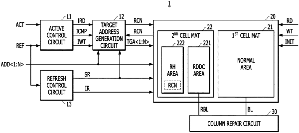
1. A memory device comprising:
a memory bank comprising a first cell mat used as a normal area and a second cell mat used as a row hammer area and a redundancy area, each of the areas being an array of memory cells;
a target address generation circuit suitable for:
saving, in the row hammer area, a count of a received address for an active operation on the memory bank by performing an internal access operation on the row hammer area during the active operation, and
setting, a particular count which satisfies a preset condition, an address corresponding to the particular count as a target address;
a refresh control circuit suitable for controlling a smart refresh operation on the target address; and
a column repair circuit suitable for repairing, when a bit line of the normal area has a defect, the bit line of the normal area with a bit line of the redundancy area.
|