| CPC G11C 11/2255 (2013.01) [G11C 11/2257 (2013.01); G11C 16/08 (2013.01); G11C 16/24 (2013.01)] | 18 Claims |
|
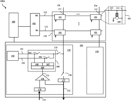
1. A memory structure comprising:
a comparator configured to receive a data output signal and a data input signal,
wherein the data input signal represents a data value to be stored in a bitcell and the data output signal represents a currently stored data value in the bitcell, and
wherein the comparator is further configured to perform a comparison of the data output signal and the data input signal and to output a data verification signal based on the comparison; and
a voltage driver configured to receive the data verification signal and to apply one specific voltage of two different voltages to at least one of a source-line and a bit-line connected to the bitcell depending upon the data verification signal,
wherein the memory structure further includes:
columns of memory cells with all memory cells in each column connected between a pair of bit and source lines for the column; and
column-specific circuitry for the columns, respectively, wherein each instance of the column-specific circuitry includes a corresponding comparator and corresponding voltage driver, and
wherein the two different voltages comprise a programming inhibit voltage and a variable programming assist voltage that is lower than the programming inhibit voltage.
|