| CPC G09G 3/3233 (2013.01) [G09G 2300/0819 (2013.01); G09G 2310/021 (2013.01); G09G 2320/0233 (2013.01); G09G 2320/0242 (2013.01); G09G 2320/0247 (2013.01); G09G 2320/045 (2013.01)] | 34 Claims |
|
1. A display panel, comprising a pixel driving circuit, wherein the pixel driving circuit comprises:
a drive transistor, a data write module, a light emission control module, a threshold compensation module and a bias adjustment module, wherein
a control terminal of the drive transistor is connected to a first node, a first terminal of the drive transistor is connected to a third node, and a second terminal of the drive transistor is connected to a second node;
the data write module is configured to provide a data signal to the drive transistor;
the light emission control module is connected in series with the drive transistor and a light-emitting element respectively and is configured to control whether a drive current flows through the light-emitting element;
the threshold compensation module is connected in series between the control terminal of the drive transistor and the second terminal of the drive transistor and configured to detect and self-compensate for a threshold voltage deviation of the drive transistor;
a first terminal of the bias adjustment module is connected to a bias signal terminal, a second terminal of the bias adjustment module is connected to the second terminal of the drive transistor, a control terminal of the bias adjustment module is connected to a first control signal terminal, and the bias adjustment module is configured to adjust, under control of a first control signal inputted through the first control signal terminal and a bias signal inputted through the bias signal terminal, a bias state of the drive transistor;
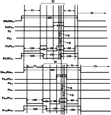
an ith pixel row and an (i+1)th pixel row form a pixel row group, and an (i+2)th pixel row and an (i+3)th pixel row form one pixel row group, a first control signal of the ith pixel row and a first control signal of the (i+1)th pixel row are each provided by a nth stage of first shift register, and a first control signal of the (i+2)th pixel row and a first control signal of the (i+3)th pixel row are each provided by a (n+1)th stage of first shift register, wherein each of i and n is a positive integer;
the data write module comprises a second transistor;
a control terminal of the second transistor is electrically connected to a second control signal terminal;
a first terminal of the second transistor is electrically connected to a data signal terminal;
a second terminal of the second transistor and the first terminal of the drive transistor are electrically connected to the third node; and
a second control signal of the ith pixel row is provided by a nth stage of second shift register, a second control signal of the (i+1)th pixel row is provided by a (n+1)th stage of second shift register, a second control signal of the (i+2)th pixel row is provided by a (n+2)th stage of second shift register and a second control signal of the (i+3)th pixel row a is provided by a (n+3)th stage of second shift register, wherein each of i and n is a positive integer and the second shift register is a shift register outputting the second control signal.
|