| CPC G09G 3/3233 (2013.01) [G09G 2300/043 (2013.01); G09G 2300/0426 (2013.01); G09G 2300/0819 (2013.01); G09G 2310/0202 (2013.01); G09G 2310/0264 (2013.01); G09G 2310/08 (2013.01)] | 19 Claims |
|
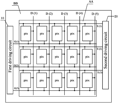
1. A display panel, comprising: a plurality of pixel circuits arranged in a matrix, a plurality of data lines, a plurality of write control lines, a plurality of compensation control lines, a first driving circuit connected to the plurality of compensation control lines, and a second driving circuit connected to the plurality of write control lines, wherein
each column of pixel circuits corresponds to one data line, and each row of pixel circuits corresponds to one write control line and one compensation control line;
the pixel circuit comprises: a driving transistor, a first switch transistor, a second switch transistor, a first capacitor and a second capacitor, wherein the first switch transistor is configured to short-circuit a gate electrode of the driving transistor and a second electrode of the driving transistor under control of a corresponding compensation control line; the second switch transistor is configured to write a signal of a corresponding data line to a first electrode of the driving transistor under control of a corresponding write control line; and the first capacitor is connected between the gate electrode of the driving transistor and a first power supply voltage end, and the second capacitor is connected between the first electrode of the driving transistor and the first power supply voltage end;
the first driving circuit is configured to output compensation control signals to each row of pixel circuits in sequence by means of the plurality of compensation control lines, and the second driving circuit is configured to output write control signals to each row of pixel circuits in sequence by means of the plurality of write control lines;
a pulse width of the compensation control signals is equal to N times a pulse width of the write control signals, the write control signals on two adjacent write control lines do not overlap, and an overlap time of the compensation control signals on two adjacent compensation control lines is equal to (N−1)/N of the pulse width of the compensation control signals, N being an integer greater than 1; and
the compensation control signals and the write control signals loaded on a same row pixel circuits overlap.
|