| CPC G09G 3/3233 (2013.01) [G09G 2300/0426 (2013.01); G09G 2300/0819 (2013.01); G09G 2300/0852 (2013.01); G09G 2310/0202 (2013.01); G09G 2310/08 (2013.01); G09G 2320/0261 (2013.01); G09G 2320/045 (2013.01)] | 18 Claims |
|
1. A display device comprising:
a plurality of data signal lines connected to a data signal line drive circuit;
a plurality of scan signal lines connected to a scan signal line drive circuit and intersecting with the plurality of data signal lines;
a plurality of pixel circuits at respective intersections of the plurality of data signal lines and the plurality of scan signal lines; and
a switching signal generation circuit, wherein
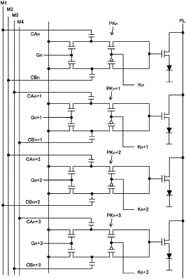
each of the plurality of pixel circuits includes:
a current-driven light-emitting element;
a drive transistor configured to control an electric current for the light-emitting element;
a switching circuit; and
a first capacitive element and a second capacitive element both connected to the switching circuit,
the switching circuit connects the first capacitive element to a control terminal of the drive transistor in a first period that falls within a single frame period and connects the second capacitive element to the control terminal of the drive transistor in a second period that falls within the single frame period and that follows the first period,
the switching circuit includes a first transistor and a second transistor,
the control terminal of the drive transistor is connected to the first capacitive element via the first transistor, and the first capacitive element is connected to a first capacitor signal line,
the control terminal of the drive transistor is connected to the second capacitive element via the second transistor, and the second capacitive element is connected to a second capacitor signal line,
the first capacitor signal line and the second capacitor signal line extend parallel to the plurality of scan signal lines,
the control terminal of the drive transistor is connected either to the first capacitive element via the first transistor or to the second capacitive element via the second transistor, by a switching signal input from the switching signal generation circuit to the switching circuit,
a first capacitor signal applied to the first capacitor signal line and a second capacitor signal applied to the second capacitor signal line are signals which toggle between a first level and a second level,
the first capacitor signal is at the first level, and the second capacitor signal is at the second level, in a select period of one of the plurality of scan signal lines that is associated with a current stage,
the first capacitor signal goes to the second level in at least a part of the first period, and
the second capacitor signal goes to the first level in at least a part of the second period.
|
|
6. A display device comprising:
a plurality of data signal lines connected to a data signal line drive circuit;
a plurality of scan signal lines connected to a scan signal line drive circuit and intersecting with the plurality of data signal lines;
a plurality of pixel circuits at respective intersections of the plurality of data signal lines and the plurality of scan signal lines;
a switching signal generation circuit;
a first main line and a second main line; and
a third main line and a fourth main line, wherein
each of the plurality of pixel circuits includes:
a current-driven light-emitting element;
a drive transistor configured to control an electric current for the light-emitting element;
a switching circuit; and
a first capacitive element and a second capacitive element both connected to the switching circuit,
the switching circuit connects the first capacitive element to a control terminal of the drive transistor in a first period that falls within a single frame period and connects the second capacitive element to the control terminal of the drive transistor in a second period that falls within the single frame period and that follows the first period,
the switching circuit includes a first transistor and a second transistor,
the control terminal of the drive transistor is connected to the first capacitive element via the first transistor, and the first capacitive element is connected to a first capacitor signal line,
the control terminal of the drive transistor is connected to the second capacitive element via the second transistor, and the second capacitive element is connected to a second capacitor signal line,
the first capacitor signal line and the second capacitor signal line extend parallel to the plurality of scan signal lines,
the control terminal of the drive transistor is connected either to the first capacitive element via the first transistor or to the second capacitive element via the second transistor, by a switching signal input from the switching signal generation circuit to the switching circuit,
the first main line is connected to the first capacitor signal line of one of the plurality of pixel circuits that is associated with a current stage,
the second main line is connected to the second capacitor signal line of the one of the plurality of pixel circuits that is associated with the current stage,
the third main line is connected to the first capacitor signal line of one of the plurality of pixel circuits that is associated with a succeeding stage, and
the fourth main line is connected to the second capacitor signal line of the one of the plurality of pixel circuits that is associated with the succeeding stage.
|