| CPC G09G 3/3233 (2013.01) [G11C 19/28 (2013.01); G09G 3/3266 (2013.01); G09G 2300/0426 (2013.01); G09G 2300/0842 (2013.01); G09G 2310/0286 (2013.01); G09G 2310/08 (2013.01); G09G 2320/0233 (2013.01); G09G 2320/0257 (2013.01); G09G 2330/021 (2013.01)] | 16 Claims |
|
1. A shift register circuit applied to a pixel driving circuit, wherein
the pixel driving circuit, comprising:
a data writing sub-circuit at least coupled to a first scanning signal terminal, a data signal terminal and a first node, the data writing sub-circuit being configured to write a data signal received at the data signal terminal into the first node under control of a first scanning signal received at the first scanning signal terminal;
a driving sub-circuit coupled to the first node, a second node and a first power supply voltage signal terminal, the driving sub-circuit being configured to drive a light-emitting device coupled to the second node to work under control of a voltage of the first node and a first power supply voltage signal received at the first power supply voltage signal terminal; and
a time control sub-circuit coupled to the first node, a second scanning signal terminal and a control signal terminal, the time control sub-circuit being configured to transmit a control signal received at the control signal terminal to the first node under control of a second scanning signal received at the second scanning signal terminal after the light-emitting device works for a preset time, so that the driving sub-circuit is turned off to control the light-emitting device to stop working; and
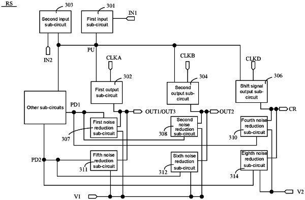
the shift register circuit comprising:
a first output sub-circuit coupled to a first clock signal terminal, a pull-up node and a first signal output terminal, the first output sub-circuit being configured to transmit a first clock signal received at the first clock signal terminal to the first signal output terminal under control of a voltage of the pull-up node, so as to transmit the first scanning signal to the first scanning signal terminal of the pixel driving circuit;
a second output sub-circuit coupled to a second clock signal terminal, the pull-up node and a second signal output terminal, the second output sub-circuit being configured to transmit a second clock signal received at the second clock signal terminal to the second signal output terminal under the control of the voltage of the pull-up node, so as to transmit the second scanning signal to the second scanning signal terminal of the pixel driving circuit after the pixel driving circuit drives the light-emitting device to work for the preset time;
a first noise reduction sub-circuit coupled to a first pull-down node, the first signal output terminal and a first voltage terminal, the first noise reduction sub-circuit being configured to transmit a voltage of the first voltage terminal to the first signal output terminal under control of a voltage of the first pull-down node;
a second noise reduction sub-circuit coupled to the first pull-down node, the second signal output terminal and the first voltage terminal, the second noise reduction sub-circuit being configured to transmit the voltage of the first voltage terminal to the second signal output terminal under the control of the voltage of the first pull-down node;
a shift signal output sub-circuit coupled to a fourth clock signal terminal, the pull-up node and a shift signal output terminal, the shift signal output sub-circuit being configured to transmit a fourth clock signal received at the fourth clock signal terminal to the shift signal output terminal under the control of the voltage of the pull-up node; and
a fourth noise reduction sub-circuit coupled to the first pull-down node, the shift signal output terminal and a second voltage terminal, the fourth noise reduction sub-circuit being configured to transmit a voltage of the second voltage terminal to the shift signal output terminal under the control of the voltage of the first pull-down node.
|