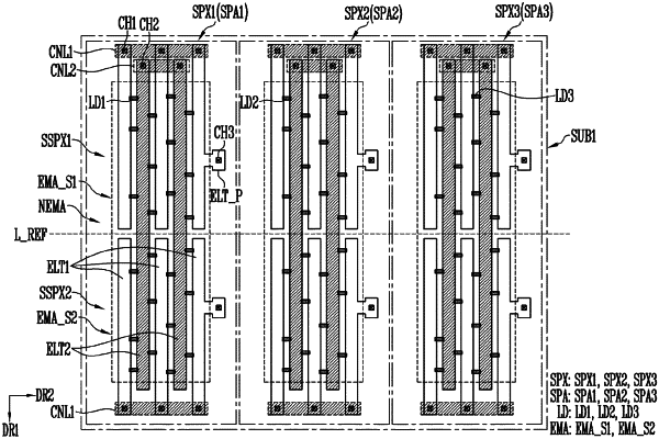
| CPC G09G 3/3233 (2013.01) [H01L 25/167 (2013.01); H01L 27/124 (2013.01); H01L 33/62 (2013.01); G09G 2300/0426 (2013.01); G09G 2300/0452 (2013.01); G09G 2300/0819 (2013.01); G09G 2300/0842 (2013.01); G09G 2320/0233 (2013.01)] | 19 Claims |

|
1. A display device comprising:
a first power line that transmits first power signal;
a second power line that transmits a second power signal;
one data line that transmits a data signal;
one scan line that transmits a scan signal; and
at least two pixels electrically connected to the first power line, the second power line, the one data line, and the one scan line, wherein
each of the at least two pixels comprises:
light emitting elements electrically connected between the first power line and the second power line; and
a first transistor that provides driving current to the light emitting elements in response to the data signal.
|