| CPC G09G 3/3233 (2013.01) [G09G 2300/0426 (2013.01); G09G 2300/0819 (2013.01); G09G 2300/0852 (2013.01); G09G 2310/08 (2013.01); G09G 2320/0233 (2013.01); G09G 2320/041 (2013.01); G09G 2320/045 (2013.01); G09G 2330/028 (2013.01)] | 19 Claims |
|
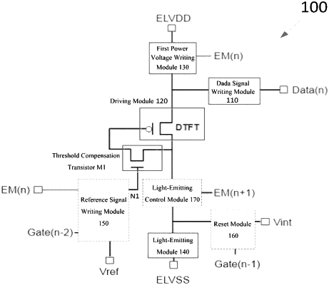
1. A pixel circuit, comprising: a data signal writing module; a driving module; a threshold compensation transistor; a first power voltage writing module; a reference signal writing module; and a light-emitting module, wherein the driving module comprises a driving transistor, wherein:
the first power voltage writing module is connected to a first light-emitting control signal terminal, a first power voltage terminal, a source of the driving transistor and a gate of the driving transistor, and the first power voltage writing module is configured to write a first power voltage signal of the first power voltage terminal to the source of the driving transistor under control of a first light-emitting control signal of the first light-emitting control signal terminal;
the data signal writing module is connected to a writing control terminal, a data signal terminal and the source of the driving transistor, and the data signal writing module is configured to transmit a data signal of the data signal terminal to the source of the driving transistor under control of a writing control signal of the writing control terminal;
the threshold compensation transistor has a gate connected to a first node, a source connected to the gate of the driving transistor and a drain connected to a drain of the driving transistor, and the threshold compensation transistor is configured to perform voltage compensation to the gate of the driving transistor in case that the first node is at an valid level;
the reference signal writing module is connected to a reference control terminal, a reference signal terminal, the first light-emitting control signal terminal and the first node, and the reference signal writing module is configured to control potential of the first node according to a reference control signal of the reference control terminal and the first light-emitting control signal of the first light-emitting control signal terminal; and
the light-emitting module has a first terminal connected to the drain of the driving transistor and a second terminal connected to a second power voltage terminal.
|