| CPC G09G 3/2092 (2013.01) [H01L 27/1251 (2013.01); H01L 27/1255 (2013.01); G09G 2300/0842 (2013.01); G09G 2310/0267 (2013.01)] | 17 Claims |

|
1. A display substrate, comprising:
a base substrate;
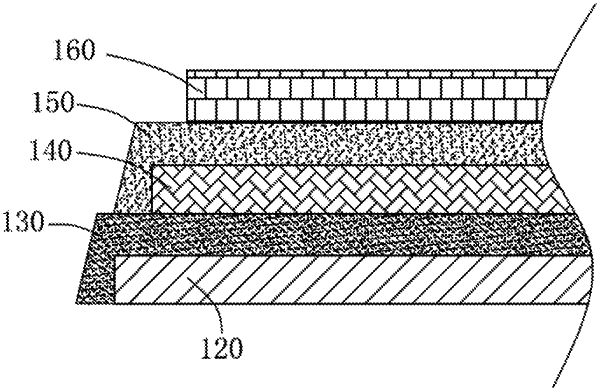
a first conductive pattern arranged on the base substrate and comprising a peripheral portion and a first portion and a second portion surrounded by the peripheral portion;
a first insulation layer arranged at a side of the first conductive pattern away from the base substrate and covering the first conductive pattern;
a second conductive pattern arranged at a side of the first insulation layer away from the base substrate, an orthogonal projection of the second conductive pattern onto the base substrate coinciding with an orthogonal projection of the first portion of the first conductive pattern onto the base substrate;
a second insulation layer arranged at a side of the second conductive pattern away from the base substrate and covering the second conductive pattern; and
a third conductive pattern arranged at a side of the second insulation layer away from the base substrate and comprising a first portion and a second portion, an orthogonal projection of the first portion of the third conductive pattern onto the base substrate being located within the orthogonal projection of the second conductive pattern onto the base substrate, an orthogonal projection of the second portion of the third conductive pattern onto the base substrate overlapping an orthogonal projection of the second portion of the first conductive pattern onto the base substrate at an overlapping region, and the third conductive pattern being electrically connected to the first conductive pattern through a via-hole at the overlapping region,
wherein the first conductive pattern, the first insulation layer, the second conductive pattern, the second insulation layer and the third conductive pattern together form a capacitor of a Gate Driver on Array (GOA) unit in the display substrate; and
the third conductive pattern and the first conductive pattern together serve as a first electrode plate of the capacitor, and the second conductive pattern serves as a second electrode plate of the capacitor;
wherein an output circuitry of the GOA unit comprises an output transistor and the capacitor, a control electrode of the output transistor is connected to a pull-up node, a first electrode of the output transistor is connected to a driving signal source, a second electrode of the output transistor is connected to a pixel driving circuitry, the first electrode plate of the capacitor is connected to the control electrode of the output transistor, the second electrode plate of the capacitor is connected to the second electrode of the output transistor, and the output transistor is configured to output a driving signal to the pixel driving circuitry under the control of a potential of a pull-up signal;
wherein the GOA unit further comprises a noise reduction circuitry, a first end of which is connected to an output end of the output circuitry and a second end of which is connected to a low level signal line, wherein the noise reduction circuitry is configured to pull down a potential at the output end of the output circuitry under the control of a potential at a pull-down node to reduce a noise;
wherein the noise reduction circuitry comprises a first noise reduction transistor and a second noise reduction transistor, the first noise reduction transistor is configured to pull down a potential at the output end of the output circuitry under the control of a first pull-down signal, the second noise reduction transistor is configured to pull down the potential at the output end of the output circuitry under the control of a second pull-down signal, the first pull-down signal and the second pull-down signal are outputted alternately.
|