| CPC G09G 3/20 (2013.01) [G09G 2300/0819 (2013.01); G09G 2300/0852 (2013.01); G09G 2300/0861 (2013.01); G09G 2310/0286 (2013.01); G09G 2310/08 (2013.01); G09G 2320/0233 (2013.01); G09G 2330/026 (2013.01)] | 20 Claims |
|
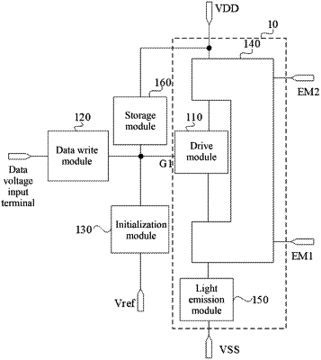
1. A pixel circuit, comprising: a drive module, a data write module, an initialization module, a light emission control module and a light emission module;
wherein the initialization module is electrically connected to a control terminal of the drive module and configured to write an initialization voltage to the control terminal of the drive module at an initialization stage;
the data write module is electrically connected to the control terminal of the drive module and configured to write a data voltage to the control terminal of the drive module at a data write stage; and
the light emission control module, the drive module and the light emission module are connected in series to form a driving branch, and the light emission control module is configured to be turned on at a light emission stage under a control of a first light emission control signal and under a control of a second light emission control signal so that the driving branch is turned on;
wherein each of the first light emission control signal and the second light emission control signal comprises a light emission signal and an extinguishing signal, wherein the light emission signal of the first light emission control signal and the light emission signal of the second light emission control signal overlap at the light emission stage, the extinguishing signal of the first light emission control signal and the extinguishing signal of the second light emission control signal overlap at the data write stage, the light emission signal of the first light emission control signal and the extinguishing signal of the second light emission control signal overlap at the initialization stage, and a period of the initialization stage within one frame is equal to an overlapping period of the light emission signal of the first light emission control signal and the extinguishing signal of the second light emission control signal before the data write stage.
|