| CPC G06F 30/392 (2020.01) | 20 Claims |
|
1. A method, comprising:
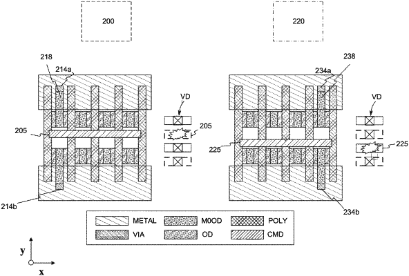
placing a base layout cell in a layout, wherein the base layout cell comprises:
first and second metal layer patterns extending in a first direction;
a plurality of active area layer patterns between the first metal layer pattern and the second metal layer pattern, wherein the plurality of active area layer patterns extends in the first direction;
a plurality of conductive gate layer patterns extending in a second direction perpendicular to the first direction and traversing over the first and second metal layer patterns and over the plurality of active area layer patterns;
a plurality of contact layer patterns extending in the second direction between two conductive gate layer patterns of the plurality of conductive gate layer patterns, wherein at least one contact layer pattern of the plurality of contact layer patterns traverses over at least one active area layer pattern of the plurality of active area layer patterns; and
a cut metal layer extending in the first direction between two active area layer patterns of the plurality of active area layer patterns, wherein the cut metal layer is between at least two conductive gate layer patterns;
connecting one or more of the first and second metal layer patterns, the plurality of active area layer patterns, the plurality of conductive gate layer patterns, the plurality of contact layer patterns to represent a first circuit; and
defining the first circuit based on a base mark of the base layout cell.
|