| CPC G06F 3/0679 (2013.01) [G06F 3/0613 (2013.01); G06F 3/0644 (2013.01); G06N 5/04 (2013.01); G11C 13/0004 (2013.01); G11C 13/0007 (2013.01)] | 20 Claims |
|
1. An apparatus comprising:
a solid state drive (SSD) device comprising:
first circuitry to:
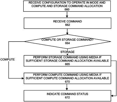
receive a configuration of at one type of command, the configuration to define an amount of media bandwidth allocated for the at one type of command,
receive a command, wherein a type of the received command is one of the at least one type of command and wherein the type of command comprises a compute command, and
assign the received command to second circuitry for execution based on the configuration, wherein the compute command is to cause processing of data read from a media and the second circuitry comprises a field programmable gate array (FPGA) and is to perform data pattern recognition, image recognition, and apply artificial intelligence and machine learning; and
third circuitry to provide a connection with the first circuitry.
|