| CPC G06F 3/0616 (2013.01) [G06F 3/0653 (2013.01); G06F 3/0679 (2013.01); G11C 29/08 (2013.01)] | 20 Claims |
|
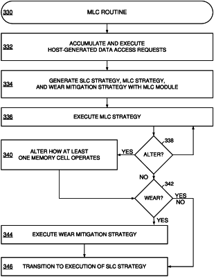
1. A method comprising:
programming a non-volatile memory unit with a first logical state in response to a first write voltage of a first hysteresis loop, as directed by a write controller;
programming the non-volatile memory unit with a second logical state in response to a second write voltage of the first hysteresis loop, the first and second logical states present concurrently in the non-volatile memory unit;
reading the first and second logical states from the non-volatile memory unit concurrently; and
testing, with a monitor circuit, the non-volatile memory unit during satisfaction of a host generated data access request to the non-volatile memory unit with an alternate read voltage selected by the monitor circuit.
|