| CPC G06F 3/0446 (2019.05) [G02F 1/13338 (2013.01); G06F 3/044 (2013.01); G06F 3/0412 (2013.01); G06F 3/0445 (2019.05); H01B 1/08 (2013.01); H05K 1/0298 (2013.01); H05K 1/0313 (2013.01); H05K 1/117 (2013.01); H05K 5/0017 (2013.01); G02F 2201/42 (2013.01)] | 16 Claims |
|
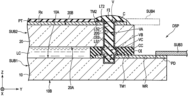
1. A conducting structure comprising:
a first layer;
a first terminal on the first layer;
a second layer overlapping the first layer via the first terminal;
a second terminal on the second layer;
a first hole which penetrates the second layer and the second terminal;
an organic insulating layer located between the first terminal and the second layer, and having a second hole connected to the first hole; and
a connecting material provided in the first and second holes to electrically connect the first terminal and the second terminal to each other, and
a detection electrode located on the second layer and connected to the second terminal, wherein
a diameter of the second hole is greater than a diameter of the first hole, and
a thickness of the second terminal is greater than a thickness of the detection electrode.
|