| CPC G06F 3/04164 (2019.05) [G06F 3/0412 (2013.01); G06F 2203/04103 (2013.01); G06F 2203/04111 (2013.01); G06F 2203/04112 (2013.01)] | 20 Claims |
|
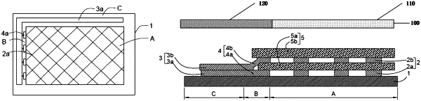
1. A touch substrate, comprising a base substrate and a touch electrode structure in a display area of the base substrate, wherein
the touch substrate further comprises a conductive structure and a wiring structure, wherein the conductive structure is in a peripheral area of the base substrate outside the display area, and comprises at least one conductive layer, and the at least one conductive layer comprises a one-piece layer of a whole layer without any pattern design, which is configured to be intended to form a lead electrically connected to a driving circuit for the touch electrode structure; and
the wiring structure is in a wiring area between the display area and the peripheral area of the base substrate and is configured to electrically connect the conductive structure to the touch electrode structure.
|