| CPC G06F 21/32 (2013.01) [G06F 3/03543 (2013.01); G06F 3/03547 (2013.01); G06F 3/044 (2013.01); G06F 3/0446 (2019.05); G06F 3/041661 (2019.05); G06F 21/44 (2013.01); G06V 40/1359 (2022.01); H01L 27/127 (2013.01); H01L 27/1255 (2013.01); G06F 2203/0336 (2013.01); G06V 40/1306 (2022.01); H01L 27/1218 (2013.01)] | 15 Claims |
|
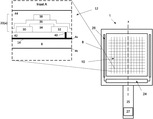
1. A pixel structure comprising a plurality of layers for providing a touch sensitive pixel of a sensing array, the layers comprising:
a thin film transistor;
a gate layer of the pixel structure comprising a gate region of the thin film transistor; and
a conductive layer deposited on a dielectric shield to be touched by an object to be sensed and arranged to provide a capacitive sensing electrode coupled to the thin film transistor,
wherein the dielectric shield provides a substrate on which the layers of the pixel structure are disposed,
wherein the thin film transistor comprises a plurality of layers deposited on the capacitive sensing electrode,
wherein the gate layer is connected to the capacitive sensing electrode.
|