| CPC G06F 12/0653 (2013.01) [G06F 12/0215 (2013.01); G11C 11/4093 (2013.01); G11C 29/12 (2013.01); H01L 25/0652 (2013.01); H01L 25/0657 (2013.01); H01L 25/18 (2013.01); G06F 2212/1016 (2013.01); G11C 2211/4062 (2013.01); H01L 2225/0651 (2013.01); H01L 2225/0652 (2013.01); H01L 2225/06506 (2013.01); H01L 2225/06513 (2013.01); H01L 2225/06517 (2013.01); H01L 2225/06541 (2013.01); H01L 2225/06562 (2013.01); H01L 2225/06586 (2013.01)] | 20 Claims |
|
1. A memory system, comprising:
a processor coupled to a first substrate;
a memory device coupled to the first substrate adjacent to the processor, the memory device including:
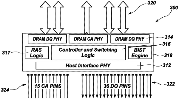
a buffer device coupled to a second substrate, the buffer device including a host interface, and a DRAM interface wherein the host interface includes at least one memory channel, and wherein the DRAM interface includes at least two sub-channels;
a stack of multiple DRAM dies coupled to the second substrate; and
circuitry in the buffer device, configured to operate the host interface at a first data speed, and to operate the DRAM interface at a second data speed, slower than the first data speed, the circuitry configured to map the at least one memory channel to the at least two sub-channels.
|