| CPC G06F 12/0646 (2013.01) [G06F 11/0727 (2013.01); G06F 11/0751 (2013.01); G06F 11/0793 (2013.01); G11C 11/407 (2013.01); G11C 29/04 (2013.01); H01L 25/0657 (2013.01); H01L 2225/06541 (2013.01)] | 21 Claims |
|
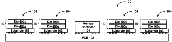
1. A memory device, comprising:
a plurality of memory dies, each memory die of the plurality of memory dies including:
command/address decoders coupled to external contacts of the memory device and configured to (a) receive command and address signals from the external contacts and (b) when enabled, to decode the command and address signals and to transmit the decoded command and address signals to other memory dies of the plurality of memory dies; and
master selection circuitry configured to enable, or disable, or both corresponding command/address decoders of a respective memory die,
wherein the command/address decoders of the plurality of memory dies are each enabled or disabled via the corresponding master selection circuitry based at least in part on differences between one or more process corners of memory dies of the plurality of memory dies.
|