| CPC G06F 12/0292 (2013.01) [G06F 3/061 (2013.01); G06F 3/064 (2013.01); G06F 3/0673 (2013.01); G06F 9/3004 (2013.01); G06F 9/3009 (2013.01); G06F 9/30145 (2013.01); G06F 9/3814 (2013.01); G06F 13/1689 (2013.01); G06F 2212/16 (2013.01)] | 7 Claims |
|
1. A memory system comprising:
a plurality of memory slices each comprising a plurality of memory tiles for storing data;
a plurality of instruction control circuits each located at one end of a respective memory slice of the plurality of memory slices, and configured to provide instructions to memory tiles of the respective memory slice, wherein the instructions are propagated sequentially over the plurality of memory tiles of the respective memory slice; and
a plurality of data lanes connecting corresponding memory tiles of the plurality of memory slices;
wherein a memory tile of a memory slice of the plurality of memory slices receives at least one instruction provided by its respective instruction control circuit during a first cycle and executes an instruction of the at least one instruction on data during a second cycle, the second cycle having a predetermined temporal relationship with the first cycle based upon an instruction type of the instruction,
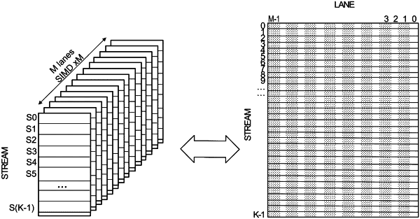
wherein each of the plurality of data lanes comprises a plurality of stream register files for storing data being transported along the data lane, each stream register file adjacent to one or more respective groups of adjacent memory slices, wherein each memory slice of the group is selectively configured to read or write to its corresponding adjacent stream register files on the plurality of data lanes.
|