| CPC G03G 15/043 (2013.01) [G03G 15/04036 (2013.01); G03G 21/1832 (2013.01); G03G 2215/08 (2013.01); G03G 2221/1609 (2013.01)] | 17 Claims |

|
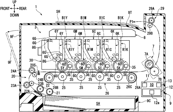
1. An image forming apparatus comprising:
a photoconductive body;
a light source configured to emit a light beam;
a deflector including a polygon mirror, the deflector being configured to deflect the light beam emitted by the light source and scan the light beam in a scanning direction;
a scanning optical system configured to image the light beam deflected by the deflector onto the photoconductive body;
a developing unit including a developing roller configured to supply developer to the photoconductive body;
an optical sensor configured to detect the light beam deflected by the deflector;
a cam configured to press the developing unit and move the developing unit to a first position where an optical path of the light beam from the scanning optical system to the photoconductive body is opened, and to a second position where the optical path is closed by a wall of the developing unit; and
a controller configured to:
when receiving a command to perform image formation, start driving the deflector;
after receiving the command to perform image formation and starting driving the deflector, when the developing unit is in the second position, cause the light source to continuously emit the light beam over an area of a single surface of the polygon mirror including an exposure scanning range in the scanning direction within which the photoconductive body is exposed to the light beam, thereby obtaining a detection signal of the light beam from the optical sensor; and
after obtaining the detection signal, control the light source to emit the light beam only within a particular range outside the exposure scanning range in the scanning direction, and thereafter control the cam to move the developing unit to the first position.
|