| CPC G03F 7/031 (2013.01) [C08G 73/1067 (2013.01); C08G 73/1071 (2013.01); G03F 7/039 (2013.01); G03F 7/0387 (2013.01); H01L 21/481 (2013.01); H01L 21/4857 (2013.01); H01L 23/3128 (2013.01); H01L 23/49822 (2013.01); H01L 23/49894 (2013.01); H01L 23/5389 (2013.01); H01L 24/24 (2013.01); H01L 24/82 (2013.01); H01L 25/18 (2013.01); H01L 21/561 (2013.01); H01L 2224/24137 (2013.01); H01L 2224/82101 (2013.01)] | 20 Claims |
|
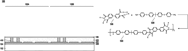
1. A method of manufacturing a semiconductor device, the method comprising:
placing a polymer material over a substrate, the polymer material comprising:
a polymer precursor, the polymer precursor comprising the following structure
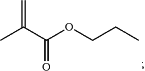
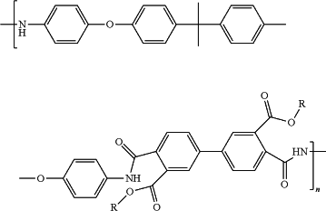 wherein n outside the brackets represents a number of the repeating unit of the structure, and wherein R represents
 a photosensitizer; and
a solvent;
patterning the polymer material; and
curing the polymer material at a temperature in a range of 200° C. to 300° C.
|