| CPC G02F 1/136222 (2021.01) [G02F 1/13439 (2013.01); G02F 1/133357 (2021.01); G02F 1/134309 (2013.01); G02F 1/136209 (2013.01); G02F 1/136286 (2013.01); H01L 27/1244 (2013.01); H01L 27/1248 (2013.01); H01L 27/1259 (2013.01); G02F 1/1337 (2013.01)] | 14 Claims |
|
1. An array substrate, comprising:
a first substrate base;
common electrode lines disposed on the first substrate base;
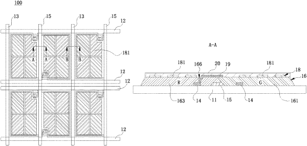
a color filter layer disposed on the first substrate base, the color filter layer comprising first color filters and second color filters adjacent to the first color filters, and the first color filters and the second color filters adjacent to the first color filters form color filter channels on the common electrode lines;
a planarization layer comprising filling portions, and the filling portions are filled in the color filter channels; and
a plurality of data lines disposed on the first substrate base, wherein the plurality of data lines is disposed parallel to and alternating with the common electrode lines, the color filter layer further comprises third color filters, and an edge of each of the third color filters and an edge of a respective one of the first color filters overlap over a corresponding one of the plurality of data lines.
|