| CPC G02F 1/13452 (2013.01) [G02F 1/13306 (2013.01); G02F 1/13456 (2021.01); G02F 1/136286 (2013.01); G09G 3/035 (2020.08); G09G 3/3685 (2013.01); H01L 23/49838 (2013.01); H01L 23/5386 (2013.01); H01L 25/50 (2013.01); H01L 27/124 (2013.01); H01L 23/4985 (2013.01); H01L 23/5387 (2013.01); H01L 25/18 (2013.01)] | 7 Claims |
|
1. A display panel, comprising:
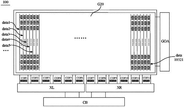
a display substrate comprising a plurality of array units, the plurality of array units being configured to control a plurality of pixel units to display an image, wherein each of the plurality of array units comprises a plurality of data lines and a plurality of pads; and
a plurality of chip on films, arranged in one-to-one correspondence with and electrically connected to the plurality of array units to drive the display substrate to display the image, wherein each of the plurality of chip on films comprises a flexible film and a driver chip, wherein,
the flexible film comprises at least a first group of lines and a second group of lines;
M lines of the first group of lines are electrically connected to pins of the driver chip to form driver lines; and
N lines of the second group of lines are not electrically connected to any pin of the driver chip, serving as nominal lines;
the plurality of array units comprise a plurality of first array units, the plurality of chip on films comprise a plurality of first chip on films; each of the first array units comprises M data lines and (M+N) pads; the M pads are connected to the M data lines respectively to form first driver pads, the N pads are not connected to any data line and serve as first nominal pads; the M driver lines of the first chip on film are arranged in one-to-one correspondence with and connected to the M first driver pads, and the N nominal lines are arranged in one-to-one correspondence with and connected to the N first nominal pads;
the plurality of array units comprise a second array unit, the plurality of chip on films comprise a second chip on film; the second array unit comprises (M−X) data lines and (M+N) pads; (M−X) pads of the second array unit are connected to the (M−X) data lines of the second array unit respectively to form second driver pads, the N pads of the second array unit are not connected to any data line and serve as first nominal pads of the second array unit; the X pads of the second array unit are disposed at left of the (M−X) second driver pads, not connected to any data line, and serve as second nominal pads; the M driver lines of the second chip on film are arranged in one-to-one correspondence with and connected to the X second nominal pads and the (M−X) second driver pads, and the N nominal lines of the second chip on film are arranged in one-to-one correspondence with and connected to the N first nominal pads of the second array unit;
the plurality of array units further comprise a third array unit, the plurality of chip on films comprise a third chip on film; the third array unit comprises (M−Y) data lines and (M+N) pads; (M−Y) pads of the third array unit are connected to the (M−Y) data lines of the third array unit respectively to form third driver pads, the N pads of the third array unit are not connected to any data line and serve as first nominal pads of the third array unit; the Y pads of the third array unit are disposed at right of the (M−Y) third driver pads, not connected to any data line, and serve as third nominal pads; the M driver lines of the third chip on film are arranged in one-to-one correspondence with and connected to the (M−Y) third driver pads and the Y third nominal pads, and the N nominal lines of the third chip on film are arranged in one-to-one correspondence with and connected to the N first nominal pads of the third array unit; and
the second array unit and the third array unit are disposed on opposite sides of the plurality of first array units; and the second chip on film and the third chip on film are disposed on opposite sides of the plurality of first chip on films.
|