| CPC G02B 6/4214 (2013.01) [G02B 6/12002 (2013.01); G02B 6/125 (2013.01); G02B 6/30 (2013.01); G02B 6/4204 (2013.01); G02B 6/4245 (2013.01); G02B 6/43 (2013.01); G02B 6/021 (2013.01); G02B 6/02038 (2013.01); G02B 6/02123 (2013.01); G02B 6/036 (2013.01); G02B 6/4256 (2013.01)] | 18 Claims |
|
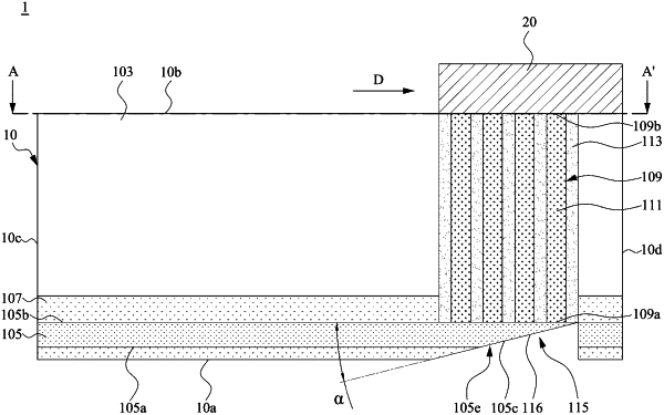
1. An optoelectronic device, comprising:
a photonic component including
an active side and a second side opposite to the active side; and
a plurality of first optical channels extending from the active side to the second side of the photonic component, wherein the photonic component has a reflective surface recessed from the active side, and projections of the plurality of first optical channels are within the reflective surface;
wherein a distance between the reflective surface and a bottom end of a first channel of the plurality of first optical channels is different from a distance between the reflective surface and a bottom end of a second channel of the plurality of first optical channels.
|