US 11,867,775 B2
Systems, devices, and methods for resistance metrology using graphene with superconducting components
Randolph Elmquist, Gaithersburg, MD (US); Albert Rigosi, Rockville, MD (US); and Mattias Kruskopf, Washington Grove, MD (US)
Assigned to Government of the United States of America, Gaithersburg, MD (US); and University of Maryland, College Park, College Park, MD (US)
Appl. No. 17/435,807
Filed by UNIVERSITY OF MARYLAND, COLLEGE PARK, College Park, MD (US); and GOVERNMENT OF THE UNITED STATES OF AMERICA, AS REPRESENTED BY THE SECRETARY OF COMMERCE, NATIONAL INSTITUTE OF STANDARDS AND TECHNOLOGY, Gaithersburg, MD (US)
PCT Filed Mar. 4, 2020, PCT No. PCT/US2020/020969
§ 371(c)(1), (2) Date Sep. 2, 2021,
PCT Pub. No. WO2020/180977, PCT Pub. Date Sep. 10, 2020.
Claims priority of provisional application 62/813,526, filed on Mar. 4, 2019.
Prior Publication US 2022/0146597 A1, May 12, 2022
Int. Cl. G01R 33/00 (2006.01); G01R 33/035 (2006.01); G01R 33/07 (2006.01); H10N 60/81 (2023.01); H10N 60/85 (2023.01)
CPC G01R 33/0052 (2013.01) [G01R 33/035 (2013.01); G01R 33/07 (2013.01); H10N 60/81 (2023.02); H10N 60/85 (2023.02)] 22 Claims
OG exemplary drawing
 
1. A quantum Hall resistance apparatus to improve resistance standards, the quantum Hall resistance apparatus comprising:
a substrate;
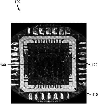
a plurality of Hall bars made of graphene electrical conduction layer, which is epitaxially grown on the substrate, each Hall bar having a plurality of first contact patterns at edges thereof;
a plurality of contacts, each including a second contact pattern and configured to connect to a corresponding first contact pattern; and
a protective layer configured to protect first contact patterns and to increase adherence between the first contact patterns and the second contact patterns,
wherein the plurality of contacts become a superconductor at a temperature lower than or equal to a predetermined temperature and under up to a predetermined magnetic flux density.