| CPC G01R 31/2884 (2013.01) [G01R 31/31715 (2013.01); G01R 31/318511 (2013.01)] | 17 Claims |
|
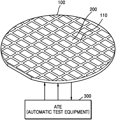
1. A wafer level test method of a stacked semiconductor chip including a plurality of core dies and a buffer die configured to provide a channel interface independent of each of the plurality of core dies that are stacked, each of the plurality of core dies including at least one semiconductor device, the wafer level test method comprising:
setting a mode register set (TMRS) bit signal allocated to indicate that a test access signal pad is not used by an external test device;
receiving master test operation signals provided by the external test device via master test pads of the buffer die;
detecting a toggling of at least one of the master test operation signals;
generating an internal master test enable signal in response to the detected toggling and the TMRS bit signal;
transmitting the internal master test enable signal via through-electrodes connected to the plurality of core dies to an internal test enable signal line of a channel selected from among a plurality of channels respectively connected to the plurality of core dies; and
performing a test operation on a semiconductor device in the selected channel, based on the internal master test enable signal,
wherein the detecting of the toggling of at least one of the master test operation signals comprises:
detecting a toggling of a second master test operation signal in an interval in which a first master test operation signal among the master test operation signals is at a certain logic level, and
wherein the first master test operation signal is different from the second master test operation signal.
|