| CPC G01R 31/2601 (2013.01) [G01R 31/2639 (2013.01); G01R 31/31725 (2013.01); G01R 31/318328 (2013.01); G01R 31/318536 (2013.01); G06F 13/4221 (2013.01); G06F 2213/0026 (2013.01)] | 20 Claims |
|
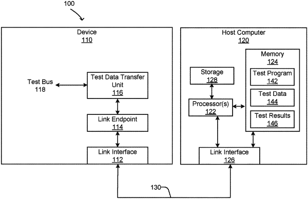
1. A method for testing a semiconductor device, comprising:
causing a clock control unit to stop transmitting clock signals to an interface circuit that resides within the semiconductor device and couples the semiconductor device to a high-speed data transfer connection;
after the clock control unit has stopped transmitting the clock signals, causing the interface circuit to be isolated from portions of the semiconductor device; and
after waiting for a first predetermined period of time to expire, causing the clock control unit to start transmitting clock signals again to the interface circuit.
|