US 11,866,598 B2
Compositions and methods including depositing nanomaterial
John R. Linton, Concord, MA (US); Peter T. Kazlas, Sudbury, MA (US); Craig Breen, Somerville, MA (US); and Seth Coe-Sullivan, Redondo Beach, CA (US)
Assigned to SAMSUNG ELECTRONICS CO., LTD., Gyeonggi-Do (KR)
Filed by SAMSUNG ELECTRONICS CO., LTD., Suwon-si (KR)
Filed on Jan. 4, 2022, as Appl. No. 17/568,204.
Application 17/568,204 is a continuation of application No. 16/440,322, filed on Jun. 13, 2019, granted, now 11,472,979.
Application 16/440,322 is a continuation of application No. 15/730,906, filed on Oct. 12, 2017, granted, now 11,214,701, issued on Jan. 4, 2022.
Application 15/730,906 is a continuation of application No. 14/531,114, filed on Nov. 3, 2014, granted, now 9,815,996, issued on Nov. 14, 2017.
Application 14/531,114 is a continuation of application No. 12/655,074, filed on Dec. 22, 2009, granted, now 8,876,272, issued on Nov. 4, 2014.
Application 12/655,074 is a continuation of application No. PCT/US2008/007901, filed on Jun. 25, 2008.
Claims priority of provisional application 60/949,306, filed on Jul. 12, 2007.
Claims priority of provisional application 60/946,090, filed on Jun. 25, 2007.
Prior Publication US 2022/0127483 A1, Apr. 28, 2022
This patent is subject to a terminal disclaimer.
Int. Cl. C09D 11/52 (2014.01); B41J 2/21 (2006.01); C09D 7/40 (2018.01); C09D 11/326 (2014.01); C09D 11/38 (2014.01); C09K 11/88 (2006.01); C09D 7/61 (2018.01); C09D 7/62 (2018.01); C09D 11/00 (2014.01); C09D 11/037 (2014.01); C09K 11/02 (2006.01); H01L 33/06 (2010.01); C08K 3/22 (2006.01); C08K 7/18 (2006.01); C08K 9/00 (2006.01)
CPC C09D 11/52 (2013.01) [B41J 2/2107 (2013.01); C09D 7/61 (2018.01); C09D 7/62 (2018.01); C09D 7/68 (2018.01); C09D 7/70 (2018.01); C09D 11/00 (2013.01); C09D 11/037 (2013.01); C09D 11/326 (2013.01); C09D 11/38 (2013.01); C09K 11/02 (2013.01); C09K 11/883 (2013.01); H01L 33/06 (2013.01); C08K 3/22 (2013.01); C08K 7/18 (2013.01); C08K 9/00 (2013.01); H01L 2933/0091 (2013.01); Y10T 29/49401 (2015.01)] 30 Claims
OG exemplary drawing
 
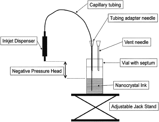
1. A method for fabricating an optical components, comprising,
depositing an ink composition comprising a nanomaterial and a non-polar organic solvent liquid vehicle over a substrate,
wherein the nanomaterial comprises a plurality of quantum confined semiconductor nanocrystals, and
wherein the nanomaterial has a solubility less than 0.001 milligrams per milliliter in the non-polar organic solvent liquid vehicle.