| CPC B29C 64/165 (2017.08) [B22F 10/00 (2021.01); B22F 10/14 (2021.01); B22F 12/37 (2021.01); B22F 12/53 (2021.01); B22F 12/55 (2021.01); B22F 12/57 (2021.01); B28B 1/001 (2013.01); B33Y 10/00 (2014.12); B33Y 30/00 (2014.12); B33Y 70/00 (2014.12); B33Y 80/00 (2014.12); H01L 21/0217 (2013.01); H01L 21/02164 (2013.01); H01L 21/02288 (2013.01); H01L 21/02532 (2013.01); H01L 21/02595 (2013.01); H01L 21/02623 (2013.01); H01L 21/288 (2013.01); H01L 21/6715 (2013.01); B22F 12/226 (2021.01); B22F 12/41 (2021.01); B22F 12/49 (2021.01); B29L 2031/34 (2013.01)] | 24 Claims |
|
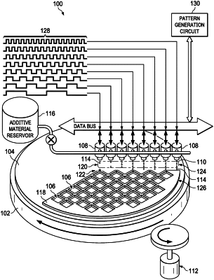
1. A method of forming an electronic device, comprising:
rotating a semiconductor wafer relative to a plurality of additive sources, the semiconductor wafer having an axis of rotation, each additive source configured to produce an amount of an additive material on the semiconductor wafer in response to a corresponding actuation signal; and
directing towards each additive source the corresponding actuation signal, thereby forming over the semiconductor wafer an additive material layer that defines a feature of the electronic device, wherein each corresponding actuation signal includes a plurality of formation actuation signals each present at an integer increment of a period corresponding to an actuation frequency having a maximum that is proportional to a distance of the corresponding additive source from the center of rotation,
wherein each actuation signal includes null actuation events, wherein each corresponding additive source omits formation of the additive material on the wafer for each null actuation event provided to that additive source.
|