| CPC B24B 37/20 (2013.01) [B24B 37/042 (2013.01); B24B 37/32 (2013.01)] | 20 Claims |
|
1. A method of forming a semiconductor wafer, the method comprising:
placing a wafer in a polishing head, the polishing head comprising:
a flexible membrane comprising a plurality of zones, each of the zones including a chamber sealed by a material of the flexible membrane;
a plurality of air passages, each of the chambers being connected to one or more of the air passages; and
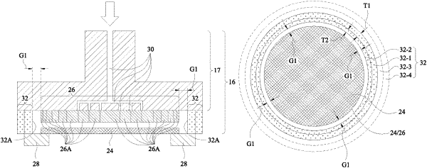
a retaining ring comprising:
a first ring having a first hardness;
a second ring within the first ring having a second hardness, wherein the second hardness is less than the first hardness by a difference greater than about 10 on Shore D scale, the second ring encircling the wafer in a plan view; and
a third ring surrounding the first ring having a third hardness, wherein the third hardness is greater than the second hardness by a difference greater than about 30 on Shore D scale, and wherein the first ring, the second ring, and the third ring are joined together to form the retaining ring; and
polishing the wafer by bringing the wafer into contact with a polishing pad.
|