| CPC B06B 1/0666 (2013.01) [H01L 28/55 (2013.01); H10B 53/30 (2023.02); H10N 15/15 (2023.02); H10N 30/06 (2023.02); H10N 30/073 (2023.02); H10N 30/085 (2023.02); H10N 30/8554 (2023.02); H10N 30/082 (2023.02); H10N 30/853 (2023.02); H10N 30/8536 (2023.02); H10N 30/8542 (2023.02); H10N 30/8548 (2023.02); H10N 30/8561 (2023.02); H10N 30/878 (2023.02)] | 12 Claims |
|
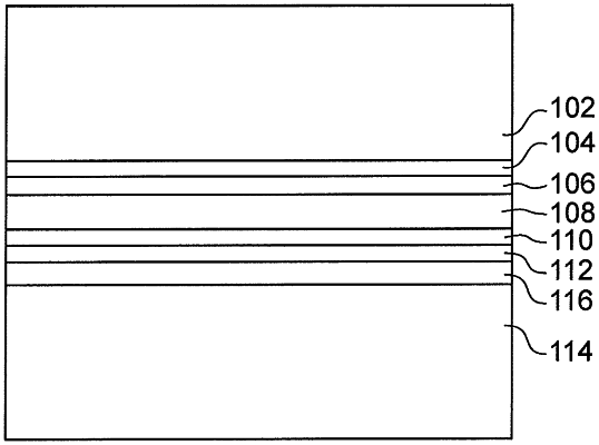
1. A method for forming an at least partially transparent device, comprising:
forming, on one face of a first substrate, a first separation layer and a second separation layer arranged one against the other and such that the first separation layer is arranged between the first substrate and the second separation layer;
forming, on the second separation layer, at least one at least partially transparent functional layer;
making the functional layer integral with a second at least partially transparent substrate, which forms a stack of different materials constituted by a first material of the first separation layer, a second material of the second separation layer, and a third material of the functional layer, each of the first, the second, and the third materials being different materials;
forming a mechanical separation at an interface between the first separation layer and the second separation layer, such that the first separation layer remains in contact with the one face of the first substrate and that the second separation layer remains integral with the functional layer;
removing the second separation layer; and
forming at least one first at least partially transparent electrode layer on the functional layer,
wherein the different materials of the stack are chosen such that the interface between the first separation layer and the second separation layer has a lowest adherence force among all interfaces of the stack, and
wherein one of the first separation layer and the second separation layer comprises SiO2 and/or silicon nitride, and the other of the first separation layer and the second separation layer comprises at least one noble metal.
|