| CPC B01L 3/502715 (2013.01) [G01N 33/48707 (2013.01); H01L 27/1214 (2013.01); B01L 2300/0645 (2013.01); B01L 2300/0819 (2013.01)] | 17 Claims |
|
1. A biological detection chip, comprising:
a first base substrate; and
a plurality of detection units arranged in an array along a row direction and a column direction on the first base substrate;
wherein each of the plurality of detection units comprises a thin film transistor and an electrode, the thin film transistor is on the first base substrate and comprises a gate electrode, a source electrode, and a drain electrode, and the electrode is on a side of the thin film transistor away from the first base substrate and is electrically connected to the drain electrode, and
the electrode is configured to carry a biological material to be detected,
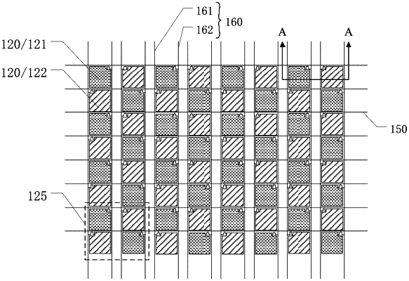
the plurality of detection units comprise stimulation units and receiving units, each of the stimulation units is configured to apply a stimulation voltage through the electrode, and each of the receiving units is configured to receive an electrophysiological signal through the electrode,
the biological detection chip further comprises: a plurality of gate lines; and a plurality of data lines arranged to intersect the plurality of gate lines,
each of the plurality of gate lines and the gate electrodes of the detection units in a same row are connected and are on a same layer, and each of the plurality of data lines and the source electrodes of the detection units in a same column are connected and are on a same layer,
the plurality of data lines comprise a first data line and a second data line, the first data line is connected with source electrodes of receiving units belonging to one column of detection units, and the second data line is connected with source electrodes of stimulation units belonging to the column of detection units,
the first data line is disposed at a first side of the column of detection units, and the second data line is disposed at a second side of the column of detection units, the second side is opposite to the first side, and
two adjacent columns of detection units are provided with one first data line and one second data line therebetween.
|