| CPC G06F 30/394 (2020.01) [H01L 27/0207 (2013.01); H01L 27/11807 (2013.01)] | 65 Claims |
|
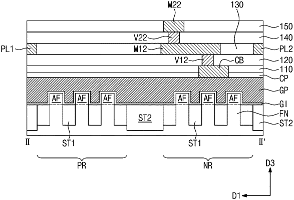
[ 20. An integrated circuit comprising:
a substrate;
a first active region;
a second active region which is spaced apart from the first active region in a first direction;
a first power line which is extending parallel to a second direction;
a second power line which is extending parallel to the second direction;
a plurality of gate patterns which are extending parallel to the first direction, wherein the plurality of gate patterns are spaced apart from each other in the second direction;
a first contact which is provided within at least one of the first active region and the second active region, and disposed on at least one of the plurality of gate patterns;
a lower metal line;
an upper metal line;
a via connecting the lower metal line to the upper metal line;
a plurality of fins extending in the second direction crossing the first direction, wherein the plurality of fins are formed on the at least one of the first active region and the second active region;
a source/drain region which is provided in portions of the at least one of the first active region and the second active region, and positioned at both sides of the at least one of the plurality of gate patterns; and
a second contact which is connected to the source/drain region;
wherein the plurality of gate patterns are provided on the plurality of fins as extending across the plurality of fins in the first direction and parallel to each other;
wherein the first contact is disposed in a first layer, the lower metal line is disposed in a second layer, and the upper metal line is disposed in a third layer;
wherein the first contact electrically connects the at least one of the plurality of gate patterns to the lower metal line;
wherein the first contact includes a first portion contacting the at least one of the plurality of gate patterns and a second portion contacting the lower metal line;
wherein the first active region and the second active region comprise a PMOSFET region and an NMOSFET region;
wherein a height of the first contact is greater than a height of the via. ]
|