| CPC H10N 70/841 (2023.02) [G06F 12/0831 (2013.01); H10B 63/80 (2023.02); H10N 70/883 (2023.02); H10N 70/8845 (2023.02)] | 16 Claims |
|
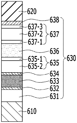
1. An electronic device comprising a semiconductor memory, the semiconductor memory comprising:
a first line;
a second line disposed over the first line to be spaced apart from the first line;
a variable resistance layer disposed between the first line and the second line;
a selection element layer disposed between the first line and the variable resistance layer; and
an electrode layer disposed between the first line and the selection element layer or between the selection element layer and the variable resistance layer,
wherein the electrode layer includes a first electrode layer and a second electrode layer, the second electrode layer including a second carbon layer containing nitrogen, the first electrode layer including a first carbon layer that contains nitrogen having a lower concentration than nitrogen contained in the second carbon layer of the second electrode layer or contains no nitrogen, the first electrode layer being interposed between the second electrode layer and the selection element layer.
|