US 11,864,474 B2
ReRAM analog PUF using filament location
Takashi Ando, Eastchester, NY (US); Franco Stellari, Waldwick, NJ (US); Guy M. Cohen, Westchester, NY (US); and Nanbo Gong, White Plains, NY (US)
Assigned to International Business Machines Corporation, Armonk, NY (US)
Filed by INTERNATIONAL BUSINESS MACHINES CORPORATION, Armonk, NY (US)
Filed on Mar. 17, 2022, as Appl. No. 17/655,184.
Prior Publication US 2023/0301212 A1, Sep. 21, 2023
Int. Cl. G11C 11/00 (2006.01); H10N 70/20 (2023.01); G11C 29/50 (2006.01); G11C 13/00 (2006.01)
CPC H10N 70/257 (2023.02) [G11C 13/004 (2013.01); G11C 29/50 (2013.01)] 20 Claims
OG exemplary drawing
 
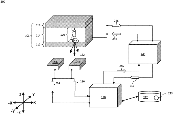
1. A semiconductor device comprising:
a resistive memory device; and
at least a first photodetector and a second photodetector positioned adjacent to the resistive memory device to allow for a spatial measurement of a filament in the resistive memory device.