| CPC H10N 60/01 (2023.02) [H10N 60/83 (2023.02)] | 20 Claims |
|
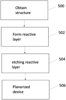
20. An apparatus for etching a substrate, comprising:
one or more reactor tools reacting a reactant with a surface of a dielectric layer so as to form a reactive layer on the dielectric layer, wherein the reactant comprises a gas or plasma, wherein:
the reactive layer comprises a chemical compound including the reactant and elements of the dielectric layer and the reactive layer comprises sidewalls defined by protrusions; and
the dielectric layer comprises the protrusions formed by the underlying nanowires; and
one or more etching tools selectively etching the protrusions laterally through the sidewalls so as to planarize the surface and remove or shrink the protrusions.
|