| CPC H10K 71/70 (2023.02) [G09G 3/006 (2013.01); H01L 22/14 (2013.01); H01L 22/32 (2013.01); H01L 27/124 (2013.01); H01L 27/1259 (2013.01); H10K 50/84 (2023.02); H10K 59/131 (2023.02); H10K 71/00 (2023.02); H10K 71/50 (2023.02); H10K 77/111 (2023.02); G09G 3/3225 (2013.01); G09G 2330/12 (2013.01); H10K 59/1201 (2023.02); H10K 2102/311 (2023.02)] | 16 Claims |
|
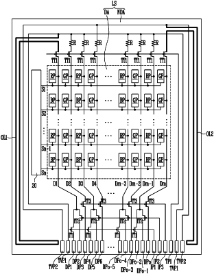
1. A display device, comprising:
a display area including a plurality of pixels electrically connected to a plurality of data lines and to a plurality of scan lines;
a first pad to receive a signal;
at least one first transistor electrically connected between one of the plurality of data lines of the display area and the first pad;
at least one outline electrically connected between the at least one first transistor and the first pad, the at least one outline being disposed in a non-display area outside of the display area;
a scan driver disposed in the non-display area and electrically connected to the plurality of scan lines,
wherein
the at least one outline is disposed outside than the scan driver in the non-display area,
the at least one outline comprises a first outline and a second outline,
the first outline go and return along an outside of each of a left side and an upper side of the display area at least once, and
the second outline is separate from the first outline and go and return along an outside of each of a right side and the upper side of the display area at least once.
|