| CPC H10K 59/65 (2023.02) [H10K 50/844 (2023.02); H10K 59/131 (2023.02); H10K 59/40 (2023.02); H10K 77/111 (2023.02)] | 20 Claims |
|
1. An organic light emitting display (“OLED”) device, comprising:
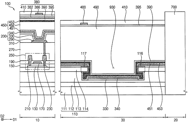
a substrate having an opening region, a peripheral region surrounding the opening region, and a display region surrounding the peripheral region, the substrate including a first groove, which has an enlarged lower portion, formed in the peripheral region and an opening formed in the opening region, the substrate includes:
a first organic film layer;
a first barrier layer on the first organic film layer;
a second organic film layer on the first barrier layer, the second organic film layer having a trench in the peripheral region; and
a second organic film layer on the first barrier layer, the second barrier layer being located on the trench and having a protruded portion that protrudes in an inner portion of the trench, the second barrier layer having an opening defined by the protruded portion;
a light emitting structure in the display region on the substrate;
a first sub-conductive pattern in the peripheral region on the substrate, the first sub-conductive pattern overlapping the protruded portion of the second barrier layer;
a second sub-conductive pattern spaced apart from the first sub-conductive pattern in the peripheral region on the substrate, the sub-conductive pattern overlapping the first groove; and
a functional module in the opening of the substrate.
|