| CPC H10K 59/131 (2023.02) [H10K 77/10 (2023.02)] | 22 Claims |
|
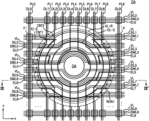
1. A display panel comprising:
a substrate including an opening area, a display area surrounding at least a part of the opening area, a first non-display area between the opening area and the display area, and a second non-display area outside the display area;
a first data line positioned at a first side relative to the opening area in a plan view of the display panel;
a second data line positioned at a second side relative to the opening area in the plan view of the display panel, wherein the opening area is positioned between the first data line and the second data line;
a first scan line;
a second scan line;
a first pixel electrically connected to each of the first data line and the first scan line;
a second pixel electrically connected to each of the first data line and the second scan line;
a third pixel electrically connected to each of the second data line and the first scan line; and
a fourth pixel electrically connected to each of the second data line and the second scan line,
a first emission control line electrically connected to the first pixel;
a first connecting section positioned on the first non-display area;
a second emission control line electrically connected to the second pixel and electrically connected through the first connecting section to the first emission control line;
a first opposite emission control line electrically connected to the third pixel;
a first opposite connecting section positioned opposite the first connecting section and positioned on the first non-display area; and
a second opposite emission control line electrically connected to the fourth pixel and electrically connected through the first opposite connecting section to the first opposite emission control line.
|