| CPC H10K 59/126 (2023.02) [G09G 3/3233 (2013.01); H10K 59/131 (2023.02); G09G 2300/0819 (2013.01); G09G 2300/0842 (2013.01); G09G 2300/0861 (2013.01); G09G 2310/0202 (2013.01); G09G 2310/08 (2013.01); G09G 2360/14 (2013.01)] | 15 Claims |
|
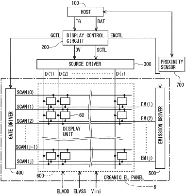
1. A display device provided with a pixel circuit including a display element driven by a current, the display device comprising:
a display unit that includes
a plurality of the pixel circuits of a plurality of rows and a plurality of columns,
a plurality of data signal lines configured to supply data signals to a plurality of the pixel circuits in corresponding respective columns,
a plurality of scanning signal lines configured to control writing of the data signals into a plurality of the pixel circuits in corresponding respective rows,
a plurality of light-emission control lines configured to control whether to supply a current to the display element included in each of a plurality of the pixel circuits in the corresponding respective rows,
a first power line configured to supply a high-level power supply voltage,
a second power line configured to supply a low-level power supply voltage, and
an initialization power line configured to supply an initialization voltage; and
a proximity sensor that includes
an emitting unit configured to emit infrared light from a back surface of the display unit, and
a light receiving unit configured to receive reflected light of the infrared light, wherein
each pixel circuit includes
a control node,
the display element including a first terminal and a second terminal connected to the second power line,
a drive transistor having a control terminal connected to the control node, a first conduction terminal, and a second conduction terminal, the drive transistor being provided in series with the display element,
a light-emission control transistor having a control terminal connected to one of the plurality of light-emission control lines, a first conduction terminal, and a second conduction terminal, the light-emission control transistor being provided in series with the display element,
a holding capacitor having one end connected to the first power line and the other end connected to the control node,
a write control transistor having a control terminal connected to one of the plurality of scanning signal lines, a first conduction terminal connected to one of the plurality of data signal lines, and a second conduction terminal connected to the first conduction terminal of the drive transistor,
a threshold voltage compensation transistor having a control terminal connected to one of the plurality of scanning signal lines, a first conduction terminal connected to the second conduction terminal of the drive transistor, and a second conduction terminal connected to the control node, and
a first initialization transistor having a control terminal connected to one of the plurality of scanning signal lines, a first conduction terminal connected to the control node, and a second conduction terminal connected to the initialization power line, and
a first light shielding unit configured to prevent a channel layer of the first initialization transistor from being irradiated with the infrared light is provided.
|