| CPC H10K 59/123 (2023.02) [G09G 3/3233 (2013.01); G09G 3/3258 (2013.01); H10K 50/805 (2023.02); H10K 59/126 (2023.02); H10K 59/1213 (2023.02); H10K 59/131 (2023.02); H10K 77/111 (2023.02); H10K 2102/311 (2023.02)] | 24 Claims |
|
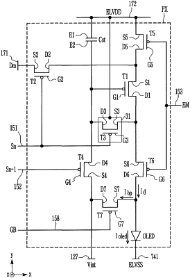
1. An organic light emitting diode (OLED) display, comprising:
a substrate;
a bottom electrode on the substrate;
a pixel; and
a scan line, a data line, and a driving voltage line connected to the pixel, wherein
the pixel includes:
an organic light emitting diode;
a switching transistor connected to the scan line; and
a driving transistor,
the bottom electrode, disposed between the switching transistor and the substrate, includes a first portion disposed in an area that overlaps the switching transistor on a plane, and
the bottom electrode is exposed by a contact hole which is disposed outside of the pixel,
wherein
the switching transistor is a third transistor including a third semiconductor layer, and
one end of the third semiconductor layer is connected to one end of a first semiconductor layer of the driving transistor and the other end of the third semiconductor layer is electrically connected to a gate electrode of the driving transistor.
|