| CPC H10K 59/1213 (2023.02) [H01L 27/1262 (2013.01); H01L 29/78603 (2013.01); H01L 29/78642 (2013.01); H01L 27/1274 (2013.01)] | 7 Claims |
|
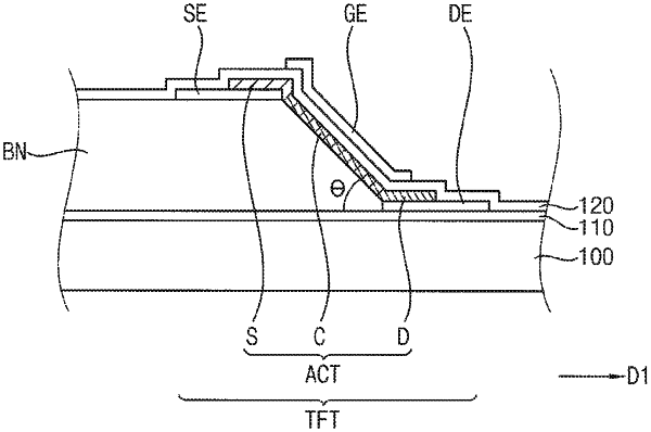
1. A method of manufacturing a thin film transistor substrate, comprising:
forming a bank having an inclined surface inclined at an angle with respect to a substrate;
forming a first electrode on the substrate, and a second electrode on the bank, the first electrode being non-overlapping with the second electrode in a plan view;
forming a preliminary active pattern including amorphous silicon on the inclined surface, the first electrode, and the second electrode;
irradiating the preliminary active pattern with an excimer laser to form an active pattern including polysilicon;
forming a gate insulting layer on the active pattern; and
forming a gate electrode on the gate insulating layer,
wherein both the first electrode and the second electrode are non-overlapping with the inclined surface in a plan view.
|