| CPC H10K 59/1213 (2023.02) [H10K 77/111 (2023.02); H01L 27/1218 (2013.01); H01L 27/1262 (2013.01); H01L 29/78603 (2013.01); H10K 59/1201 (2023.02); H10K 2102/311 (2023.02)] | 10 Claims |
|
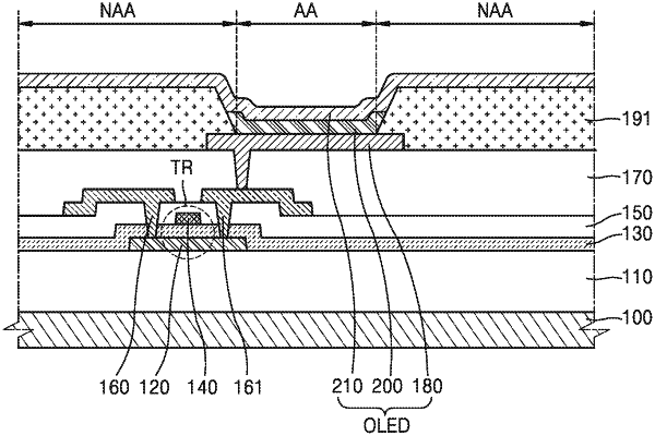
1. A thin film transistor (TFT) substrate, comprising:
a substrate;
an active layer disposed on the substrate;
a buffer layer disposed between the substrate and the active layer, the buffer layer including a first buffer layer disposed between the active layer and the substrate to direct contact with the active layer, and a second buffer layer disposed between the substrate and the first buffer layer;
a source electrode; and
a drain electrode,
wherein each of the first buffer layer and the second buffer layer includes an inorganic insulating layer and an area ratio of a peak corresponding to an N—H bond in the buffer layer is 0.5% or less based on a total peak area in a Fourier transform infrared spectroscopy (FTIR), and
wherein contents of a compound having the N—H bond in the first buffer layer decreases when a distance from an interface between the first buffer layer and the active layer increases.
|